


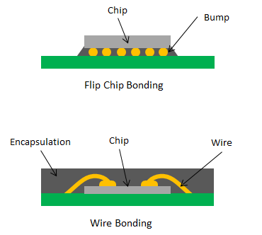
Flip Chip Bonding
In contrast to the wire bonding process, where metal wires are used to electrically connect the integrated circuit to the board with the electrode on the top, the flip-chip method places the electrode on the bottom, allowing for direct mounting onto the circuit board. This is why it is called “flip-chip.”
Compared to wire bonding, flip-chip has the advantage of shorter wiring, making it ideal for circuits in devices that require compact, slim designs, or circuits where electrical characteristics are critical. Additionally, since the electrodes are on the underside of the chip, there is no need for resin encapsulation to protect the electrodes on the package top.
We provide a complete flip-chip bonding service, including the design and production of custom tooling optimized for your product specifications. We can accommodate prototype development, small volume production, and short lead times, offering flexible solutions tailored to your needs.
Evaluation of Flip Chip
We offer a variety of evaluations, including bond strength testing of the integrated circuit and substrate using a bonding tester, bump misalignment checks using X-ray transmission equipment, and cross-sectional observations of the bond interface through cross-sectional polishing.
Shear Strength Test
The tool attached to the load sensor descends to the substrate surface, and the device detects the substrate surface and stops the descent. The tool then rises to the set height from the detected substrate surface, and the load at the moment of bond failure is measured as the tool presses on the bond interface.
X-ray inspection: Checking bump misalignment
We provide bump misalignment verification using X-ray transmission equipment.
Bonding State Verification
We use polishing equipment to slice the cross-section of the joint between the integrated circuit and the substrate for observation, photography, and measurement. We check for the condition of the alloy layer (intermetallic compounds) as well as any cracks, voids, or defects in the bump joints. By physically preparing a cross-section of the sample, we are able to observe fine abnormalities that may be difficult to detect with non-destructive testing and examine the internal structure of parts that cannot be penetrated by X-rays.
Equipment Lineup of Flip Chip
- i-Cube Series C4
We will solve your problems.
We specialize in handling highly confidential products and expensive materials, and we respond to our customers' needs in various ways. With the expertise gained from over 2,500 prototype projects, we can effectively solve your problems. We are also capable of handling small-batch production and accept orders starting from just one unit. Please feel free to reach out to us with any concerns or inquiries.
With the expertise gained from over 2,500 prototype projects, we provide comprehensive support to our customers
-
 Capable of both automated and manual assembly
-
Trusted with all semiconductor-related tasks
-
Collaborating with customers from product development onwards
-
Customizing products based on customer specifications
-
Offering one-stop service from product development to mass production, including material procurement
-
Treating custom products as if they were standard items