


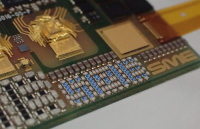
Surface Mount Technology
The Surface Mount Technology (SMT) process involves applying solder paste to the electrodes of a circuit board using specialized equipment, then mounting electronic components such as IC chips (Surface Mount Devices, SMD) onto the board. After this, the board is heated in a furnace to bond and fix the components.
We also offer post-surface-mount services such as automatic visual inspection. Additionally, we are capable of supporting prototype development, small-volume production, and short lead times.
Introduction to the Surface Mount Technology Process
The surface mounting process can be divided into four stages: 1) Solder Paste Printing, 2) Component Placement, 3) Reflow Soldering, and 4) Cleaning. The product flows in the sequence of 1) → 2) → 3) → 4).
1)Solder Paste Printing
The solder paste printing process involves applying “cream solder,” which maintains a creamy consistency at room temperature, to the electrodes on the PCB.
Cream solder is a mixture of fine solder particles and flux (a soldering aid) that is kneaded together.
Using a metal mask, solder is printed only on the electrodes of the PCB, ensuring that it is not applied to unwanted areas.
Since the application conditions of cream solder can vary due to external factors such as temperature, humidity, and viscosity, the design of the metal mask and the selection of the cream solder involve our expertise and know-how.
2)Component Placement
The mounting process involves placing electronic components onto the substrate that has been coated with cream solder.
The electronic components are supplied in tape form and are mounted to the specified locations according to a programmed process.
Barcode management of the electronic components and the use of feeders—specialized cassettes that hold the taped components—help prevent defects caused by incorrect component placement.
3)Reflow Soldering
The reflow process is where the mounted electronic components are soldered by heating.
Heat is applied to the substrate with mounted components, melting the cream solder to bond it with the components. Once the solder cools, it solidifies, fixing the components in place.
To ensure the solder melts correctly, SME controls the rate of temperature increase and heating time, working to prevent issues such as solder cracks and voids.
5)Cleaning
After soldering, flux residues may be cleaned from the PCB to prevent corrosion or component damage. This cleaning process can be performed using automated systems or manually.
The technology of Surface Mount Technology (SMT)
Our surface mount technology not only allows for component placement on both sides of the PCB but also enables the mounting of electronic components in a 90-degree upright position. Additionally, we can support high-density mounting and narrow-pitch specifications for PCB assembly.
We can handle electronic components starting from 03015 size and are equipped to work with supply forms such as reels, tape cuts, and trays. The substrates we can work with include ceramic boards, glass-epoxy boards, and flexible printed circuit boards (FPC).
・Other materials may also be handled upon request.
Evaluation of Surface Mount Technology
We use Automated Optical Inspection (AOI) systems to check for unmounted components, solder wetting conditions, and incorrect component orientation or placement. Additionally, we conduct void detection using X-ray inspection equipment and shear strength measurements using bonding testers.
Unmounted components, component orientation, and incorrect component placement
We use Automated Optical Inspection (AOI) systems to check whether the correct electronic components are placed in the correct positions and to ensure there are no missing components. Additionally, we can also verify the solder fillet quality.
Shear Strength Test
The tool attached to the load sensor descends to the surface of the PCB, and the system detects the surface, stopping the descent. The tool then rises to the preset height above the detected PCB surface, and the load is measured when the tool pushes and breaks the joint.

Void detection
We perform void detection of the solder using X-ray inspection equipment.
Bonding condition inspection
We use polishing equipment to cut the cross-section of the junction between the integrated circuit and the PCB, allowing for observation, photography, and measurement. We check the condition of the alloy layer (intermetallic compounds) as well as detect bonding defects such as cracks or voids in the solder layer.
Since this method physically exposes the cross-section of the sample, it allows for the observation of fine abnormalities that may be difficult to detect with non-destructive testing, and it also enables the inspection of components whose internal details cannot be viewed through X-ray penetration.
Underfill Equipment Lineup
1)Solder Paste Printing
- YCP-10
- SP60P-M
- MK-878SV
2)Component Placement
- YSM-10
- CM402
- CM602
3)Reflow Soldering
- NJ0611M-82
- XCA-645PC
- TNP25-537
- ANUR925
We will solve your problems.
We specialize in handling highly confidential products and expensive materials, and we respond to our customers' needs in various ways. With the expertise gained from over 2,500 prototype projects, we can effectively solve your problems. We are also capable of handling small-batch production and accept orders starting from just one unit. Please feel free to reach out to us with any concerns or inquiries.
With the expertise gained from over 2,500 prototype projects, we provide comprehensive support to our customers
-
 Capable of both automated and manual assembly
-
Trusted with all semiconductor-related tasks
-
Collaborating with customers from product development onwards
-
Customizing products based on customer specifications
-
Offering one-stop service from product development to mass production, including material procurement
-
Treating custom products as if they were standard items