


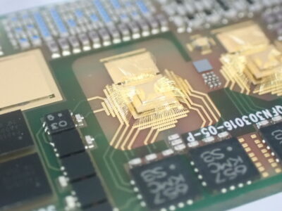
Die Bonding
The die bonding process involves adhering semiconductor devices, which are divided into individual pieces through wafer dicing, to printed circuit boards, lead frames, flexible substrates, etc., using die bonding materials such as silver paste, insulating adhesives, or DAF (Die Attach Film).
By selecting die bonding materials with excellent thermal conductivity and designing specialized tools (such as push-up pins, transfer pins, and die collets) to reduce the load on semiconductor devices, we provide die bonding services tailored to meet our customers’ needs. We offer a range of services, from fully automated die bonding using die bonding equipment to manual (hand assembly) options.
We can also accommodate on-site work with customer presence, so please feel free to contact us for any inquiries.
The technology of Die Bonding
Our die bonding technology is capable of handling semiconductor elements as small as 0.15mm in diameter. The die bonding materials we handle include silver paste, insulating adhesives, metal sintered materials, and DAF (Die Attach Film). We also offer stack bonding and die bonding on both sides of the substrate.
Other materials are also available upon request.
Evaluation of Die Bonding
We offer semiconductor device and substrate bonding strength testing using a bonding tester, cross-sectional observation of the bonding area through polishing, and void observation via X-ray inspection.
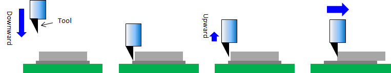
Shear Strength Test
The tool attached to the load sensor descends until it reaches the surface of the substrate, at which point the device detects the substrate surface and stops the descent. The tool then rises to a preset height above the detected surface, and the load applied at the point of breaking during the bonding is measured.
Bonding State Verification
Using a polishing device, we grind the cross-section of the joint between the semiconductor device and the substrate for observation, imaging, and measurement. We check for any bonding defects such as cracks or voids.
Since the cross-section of the sample is physically revealed, it allows us to observe minute abnormalities that are difficult to detect with non-destructive testing methods, as well as inspect the interior of components that cannot be penetrated by X-rays.
Equipment Lineup of Die Bonding
- BESTEM-D01 Series
- BESTEM-D10 Serie
- DM-60H
- STC-500
We will solve your problems.
We specialize in handling highly confidential products and expensive materials, and we respond to our customers' needs in various ways. With the expertise gained from over 2,500 prototype projects, we can effectively solve your problems. We are also capable of handling small-batch production and accept orders starting from just one unit. Please feel free to reach out to us with any concerns or inquiries.
With the expertise gained from over 2,500 prototype projects, we provide comprehensive support to our customers
-
 Capable of both automated and manual assembly
-
Trusted with all semiconductor-related tasks
-
Collaborating with customers from product development onwards
-
Customizing products based on customer specifications
-
Offering one-stop service from product development to mass production, including material procurement
-
Treating custom products as if they were standard items